EU Meetup February 13, 2018
Emiliania huxleyi, the reference species for coccolithophore studies, is contrasted with a range of other species spanning the biodiversity of modern coccolithophores. All images are scanning electron micrographs of cells collected by seawater filtration from the open ocean. (A to N) Species illustrated: (A) Coccolithus pelagicus, (B) Calcidiscus leptoporus, (C) Braarudosphaera bigelowii, (D) Gephyrocapsa AQ53 oceanica, (E) E. huxleyi, (F) Discosphaera tubifera, (G) Rhabdosphaera spinifera, (H) Calciosolenia murrayi, (I) Umbellosphaera irregularis, (J) Gladiolithus flabellatus, (K and L) Florisphaera profunda, (M) Syracosphaera pulchra, and (N) Helicosphaera carteri. Scale bar, 5 mm. Credit: Fanny M. Monteiro et al. Sci Adv 2016;2:e1501822
Read more at: https://phys.org/news/2016-07-calcification-future-ocean.html#jCp
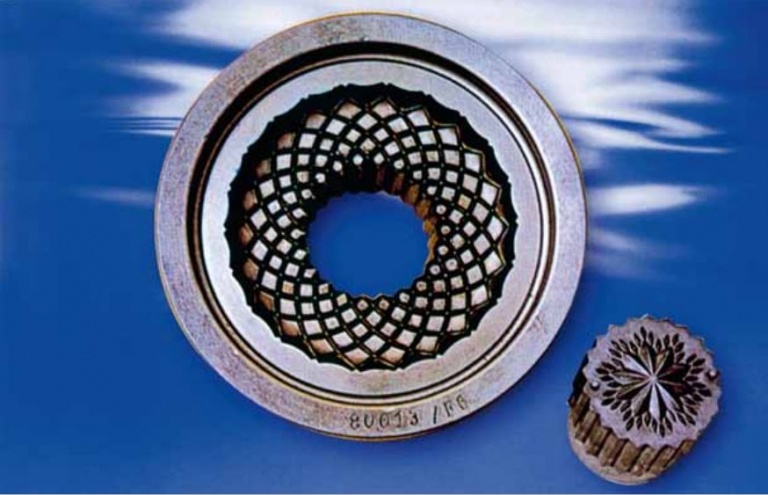
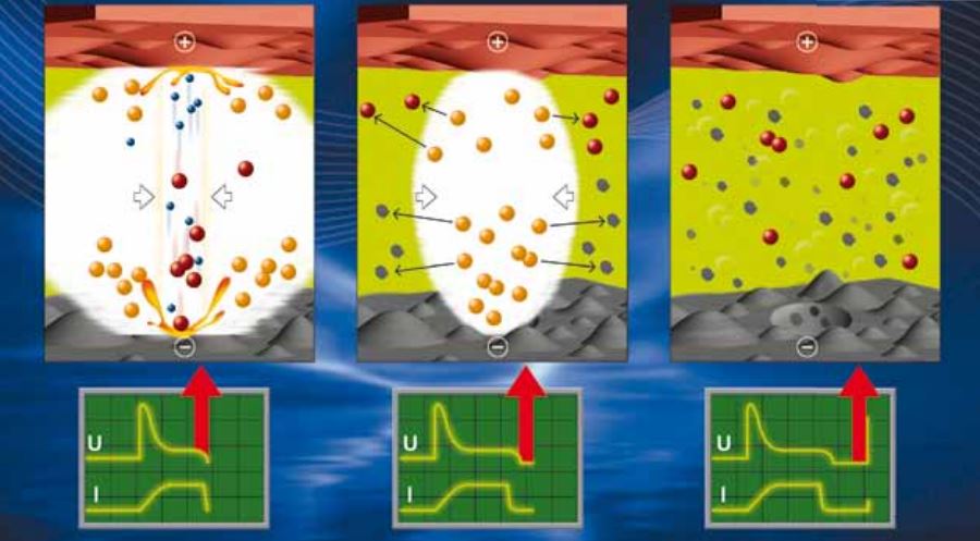
Spark erosion dieletrics
Types of plasma etching
Pressure influences the plasma etching process. For plasma etching to happen, the chamber has to be under low pressure, less than 100 Pa. In order to generate low-pressure plasma, the gas has to be ionized. The ionization happens by a glow charge. Those excitations happen by an external source, which can deliver up to 30 kW and frequencies from 50 Hz (dc) over 5–10 Hz (pulsed dc) to radio and microwave frequency (MHz-GHz).[2][9]
Microwave plasma etching
Microwave etching happens with an excitation sources in the microwave frequency, so between MHz and GHz. One example of plasma etching is shown here.[10]
A microwave plasma etching apparatus. The microwave operates at 2.45 GHz. This frequency is generated by a magnetron and discharges through a rectangular and a round waveguide. The discharge area is in a quartz tube with an inner diameter of 66mm. Two coils and a permanent magnet are wrapped around the quartz tube to create a magnetic field which directs the plasma.
Hydrogen plasma etching
On form to use gas is the plasma etching is hydrogen plasma etching. Therefore, an experimental apparatus like this can be used:[5]
Applications
Plasma etching is currently used to process semiconducting materials for their use in the fabrication of electronics. Small features can be etched into the surface of the semiconducting material in order to be more efficient or enhance certain properties when used in electronic devices.[3] For example, plasma etching can be used to create deep trenches on the surface of silicon for uses in microelectromechanical systems. This application suggests that plasma etching also has the potential to play a major role in the production of microelectronics.[3] Similarly, research is currently being done on how the process can be adjusted to the nanometer scale.[3]
Hydrogen plasma etching, in particular, has other interesting applications. When used in the process of etching semiconductors, hydrogen plasma etching has been shown to be effective in removing portions of native oxides found on the surface.[5] Hydrogen plasma etching also tends to leave a clean and chemically balanced surface, which is ideal for a number of applications.[5]








 WRC VS. THUNDERBOLTS